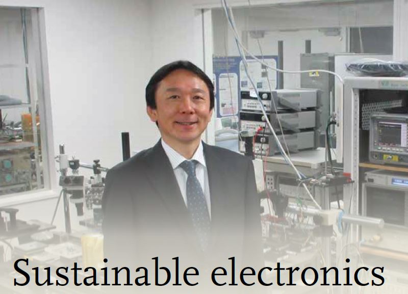
Prof. Dr. Haruichi KANAYA W2-456
Department of Electronics, Graduate School of Information Science and Electrical Engineering, Kyushu University. Nishi-ku Motooka 744,
Fukuoka city, Fukuoka, Japan
(Post Code: 819-0395)
E-mail: kanaya


Radio-Frequency Integrated Circuits (RFIC) & Microwave Communication Device Laboratory
Find us at

Research Overview
 Source: Impact, Volume 2019, Number 10, December 2019, pp. 87-89(3)
Center for Nation-Wide Cooperative Research on ICT FY 2021 RIEC Annual Meeting on Cooperative Research Projects “Compass for Next-Gen ICT” poster here.
Introduction

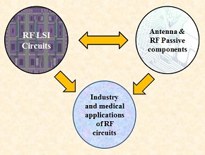
In this laboratory,we are now focusing our researches on the following areas: (1) High speed, high linearity and low noise system LSI components for wireless communications systems. (2) Wideband RF front-end components for ultra-wideband (UWB) applications. (3) Digital Radio or Digital RF Processor and its system components i.e. Digitally assisted RF/Analog circuits such as ADPLL (All-digital phase locked loop), DCO (digitally-controlled oscillators), sampling mixers, digital controlled PA, LNA etc. for Software defined radio or other reconfigurable applications. (4) Electrically small antennas for narrow band and UWB applications. (5) Interconnection and packaging technology of a chip to an antenna to reduce parasitic components. Further details on our research, please click here.
A tour of our laboratory - Open campus for high school students
Campus tour is offered annually to the high school students in Japan. Open campus give students the opportunity to meet academic staff, tour campus and learn more about major and programs offered by Kyushu University.
At the start of the tour, Prof. Dr. Kanaya gave students an idea about the scope of research in our laboratory and applications in wireless and cellular communications. In addition, the basic concept of building blocks in RF system and the circuit design of analog/RF ICs for wireless communication were introduced to the students. The tour concludes with the demonstration of the prototype co-developed by our laboratory and industry. Various methods of measurements were conducted to show the magnitude and phase from the output of the device as a function of frequency.
This tour offers a glimpse into the collaborative research efforts between academia and industry to overcome challenges in a rapidly changing world of wireless and mobile communications system.
Latest news
- 20.12.2019 Takigawa, Yamashita, and Nakashima attended Bio4Apps2019. Photographs
- 07.12.2019 Kai, Hatanaka, and Ide attended 21st Electronics Packaging Technology Conference. Photographs
- 29.11.2019 Nakashima and Yamashita attended Innovative Industry Fair for E x E Solutions. Photographs
- 29.09.2019 Nakashima and Yamashita attended 72th Joint Conference of Electrical and Electronics Engineers in Kyushu. Photographs
- 07.04.2017 Start of 2017/18 Academic Sem. I